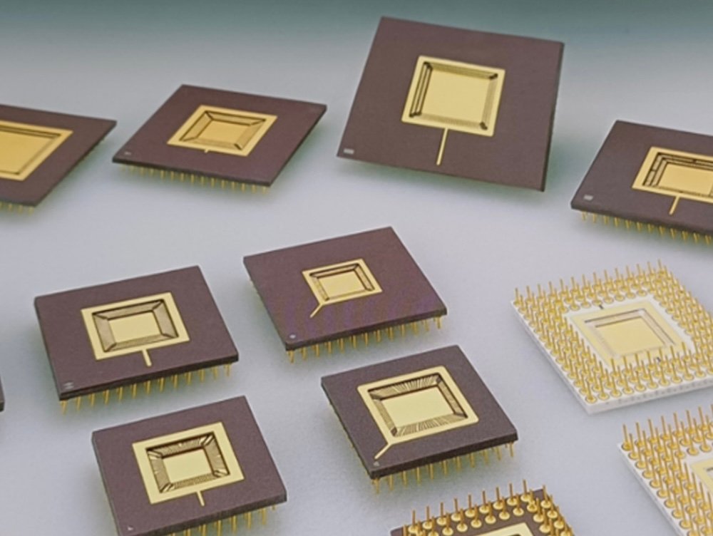
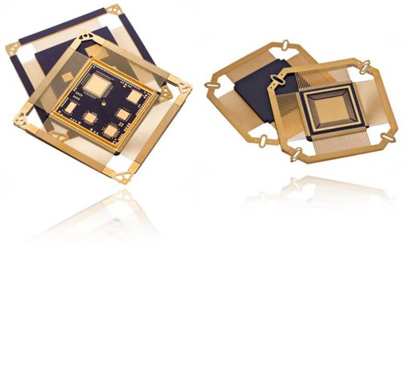
Ceramic PGA
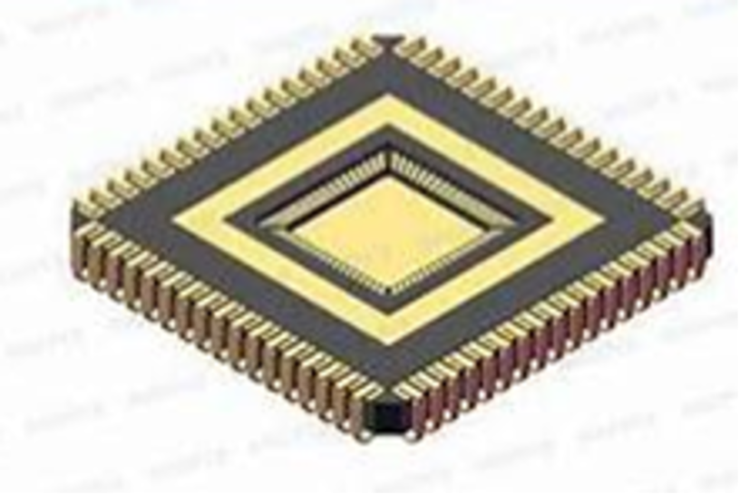
Ceramic CQFP
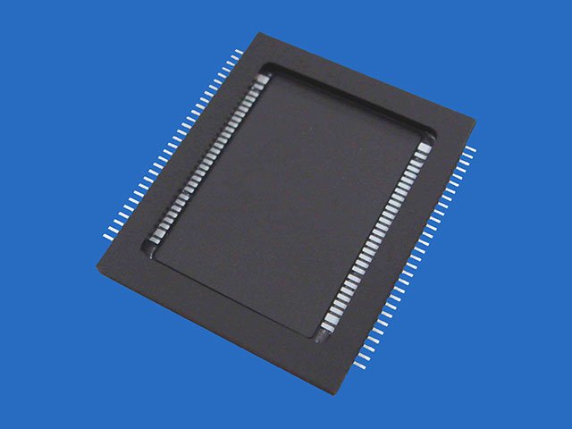
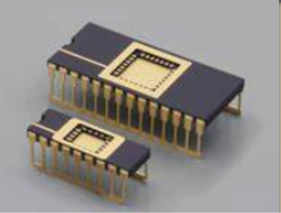
Ceramic Dual Inline Package
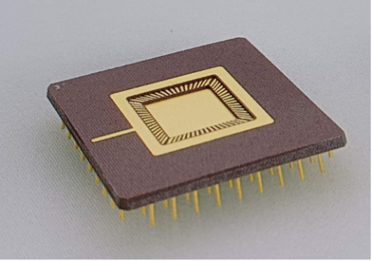
Ceramic CQFJ
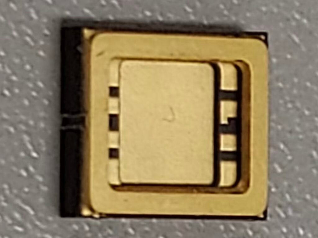
Ceramic LCC Package
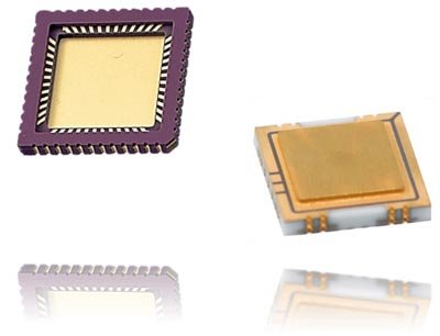
Ceramic SMD Packages